
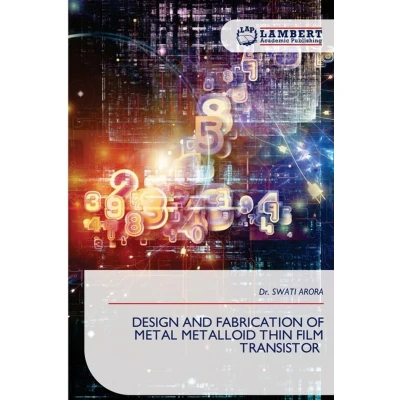
DESIGN AND FABRICATION OF METAL METALLOID THIN FILM TRANSISTOR
Uitgelicht

|
42,99 |
Naar shop
|

|
42,99 |
Naar shop
|

|
48,99 |
Naar shop
|
| VERGELIJK ALLE AANBIEDERS (3) | ||
 Beschrijving
Bol
In the work, Metal and Metalloid fabricated on the glass substrate as thin film samples and electrical behavior has found similar to thin film Field Effect Transistor. Metal (Al/Cu) contact and metalloid (Se) channel have been used as a Field Effect Transistor on the glass substrate by depositing the source, drain and top-gate metal contacts. The flow of carriers from the source to drain can be controlled with Schottky metal gate. The channel current has been controlled by depletion layer of variable width through metal contact and thickness of the conducting channel has been modulated. The source and drain of the FET structure were defined by the metal layers of Al, or Cu were sequentially deposited on the Se in the defined contact patterns by thermal evaporation by employing vacuum coating unit. The their electrical properties were determined. The device is used to control the current between drain and source at the different potential between gate and source (VGS), inducing free charge accumulation at metal-semiconductor junction. Thin Films of aluminum selenide has been annealed at 50°C, 100°C further confirmed by X-Ray Diffraction and optical spectroscopy.


 Beschrijving
(1)
Beschrijving
(1)
In the work, Metal and Metalloid fabricated on the glass substrate as thin film samples and electrical behavior has found similar to thin film Field Effect Transistor. Metal (Al/Cu) contact and metalloid (Se) channel have been used as a Field Effect Transistor on the glass substrate by depositing the source, drain and top-gate metal contacts. The flow of carriers from the source to drain can be controlled with Schottky metal gate. The channel current has been controlled by depletion layer of variable width through metal contact and thickness of the conducting channel has been modulated. The source and drain of the FET structure were defined by the metal layers of Al, or Cu were sequentially deposited on the Se in the defined contact patterns by thermal evaporation by employing vacuum coating unit. The their electrical properties were determined. The device is used to control the current between drain and source at the different potential between gate and source (VGS), inducing free charge accumulation at metal-semiconductor junction. Thin Films of aluminum selenide has been annealed at 50°C, 100°C further confirmed by X-Ray Diffraction and optical spectroscopy.
 Productspecificaties
 Prijshistorie
* Prijshistorie bevat geen data van Amazon, Amazon Marketplace.
Prijzen voor het laatst bijgewerkt op:
 Gerelateerde resultaten


